Xiamen Tmax Battery Equipments Limited was set up as a manufacturer in 1995, dealing with Laboratory equipments, technology, etc. We have total manufacturing facilities of around 2, 000 square meters and more than 100 staff. Owning a group of experie-nced engineers and staffs, we can bring you not only reliable products and technology, but also excellent services and real value you will expect and enjoy.
Wafer Sputtering Coater: Advanced Thin-Film Deposition Equipment for Semiconductor and Materials Research
Overview
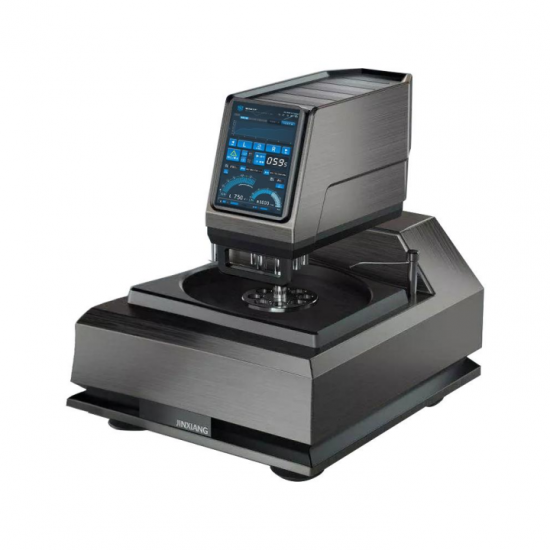
A Wafer Sputtering Coater is a high-precision vacuum deposition system designed to deposit thin films onto semiconductor wafers and other flat substrates using sputtering technology. It is one of the most important pieces of equipment in semiconductor fabrication, microelectronics, MEMS (Micro-Electro-Mechanical Systems), optoelectronics, solar cell manufacturing, battery research, and advanced materials development. By utilizing plasma-generated ions to bombard a target material, the system ejects atoms from the target, which are then deposited uniformly onto the wafer surface, forming thin films with exceptional adhesion and controlled thickness.
Modern Wafer Sputtering Coater systems integrate sophisticated vacuum technology, magnetron sputtering sources, substrate rotation mechanisms, programmable process control, and real-time monitoring to achieve highly reproducible coating results. They support a wide variety of target materials, including metals, alloys, oxides, nitrides, and composite materials, making them indispensable for both laboratory research and industrial-scale manufacturing.
With the continuous miniaturization of electronic devices and the growing demand for advanced functional materials, wafer sputtering coaters have become essential tools for producing high-quality thin films with precise electrical, optical, and mechanical properties.
---
Key Characteristics
A high-performance Wafer Sputtering Coater offers several advanced features that ensure consistent thin-film deposition and superior coating quality.
High Deposition Precision
The equipment enables precise control of coating thickness, ranging from a few nanometers to several micrometers. Accurate deposition control is critical for semiconductor devices, integrated circuits, and optical coatings where film thickness directly affects device performance.
Excellent Film Uniformity
Rotating substrate holders, optimized target geometry, and controlled plasma distribution ensure highly uniform film deposition across the entire wafer surface, including large-diameter wafers.
High Vacuum Environment
The sputtering chamber operates under high or ultra-high vacuum conditions, significantly reducing contamination and enabling the production of dense, high-purity thin films with excellent adhesion.
Multiple Sputtering Modes
Modern systems support various sputtering techniques, including:
DC Magnetron Sputtering
RF Magnetron Sputtering
Pulsed DC Sputtering
Reactive Sputtering
Co-sputtering
Multi-target Sequential Deposition
These options allow users to deposit conductive, insulating, and compound materials with high flexibility.
Intelligent Automation
Programmable control systems automatically regulate vacuum pressure, gas flow, sputtering power, substrate temperature, deposition time, and film thickness. Automated recipe management improves repeatability while minimizing operator intervention.
Flexible Substrate Compatibility
A Wafer Sputtering Coater can accommodate silicon wafers, glass, sapphire, quartz, ceramic substrates, metal foils, polymer films, and other specialized materials used in advanced research.
---
Sputtering Process
The operation of a Wafer Sputtering Coater involves several precisely controlled stages to ensure high-quality thin-film formation.
Chamber Preparation
The wafer is securely mounted onto the substrate holder, and the selected sputtering target is installed inside the vacuum chamber. The chamber is evacuated using mechanical and turbomolecular pumps to achieve the required base vacuum.
Plasma Generation
An inert gas, typically argon, is introduced into the chamber. When electrical power is applied to the sputtering target, the argon atoms become ionized, forming a stable plasma.
Target Sputtering
Positively charged argon ions are accelerated toward the negatively charged target material. The energetic ion bombardment ejects atoms from the target surface through momentum transfer.
Thin-Film Deposition
The sputtered atoms travel through the vacuum chamber and condense onto the wafer surface, forming a dense and uniform thin film. Process parameters such as gas pressure, sputtering power, substrate temperature, and deposition time are carefully controlled to achieve the desired film characteristics.
Reactive Deposition (Optional)
For compound films such as oxides or nitrides, reactive gases including oxygen or nitrogen are introduced during deposition, allowing the formation of functional ceramic coatings.
Cooling and Unloading
After deposition, the wafer is allowed to cool under vacuum or an inert atmosphere before being removed for subsequent processing or characterization.
Intelligent Grinding Polishing Machine
Applications
The versatility of a Wafer Sputtering Coater enables its use across numerous high-technology industries and research fields.
Semiconductor Manufacturing
Thin films deposited by sputtering are widely used for:
Conductive interconnects
Diffusion barriers
Contact layers
Seed layers
Metal gates
Packaging materials
MEMS Fabrication
Micro-electromechanical systems require precise thin-film coatings to fabricate sensors, actuators, pressure sensors, accelerometers, and microfluidic devices.
Optoelectronics
Wafer sputtering coaters are used to produce:
Transparent conductive films
Optical filters
Anti-reflective coatings
Reflective mirrors
OLED electrodes
Photodetector layers
Solar Cell Production
Thin-film photovoltaic devices utilize sputtered coatings for transparent conductive oxides, buffer layers, absorber layers, and back contacts.
Battery Research
Researchers use wafer sputtering systems to deposit:
Thin-film solid electrolytes
Lithium metal layers
Current collectors
Protective coatings
Electrode interface layers
These coatings support the development of advanced lithium-ion and solid-state batteries.
Materials Science
Universities and research laboratories employ wafer sputtering coaters to investigate nanomaterials, magnetic films, superconductors, catalysts, and multifunctional thin-film materials.
---
Advantages
A Wafer Sputtering Coater offers numerous benefits that make it indispensable for precision thin-film deposition.
Exceptional Film Quality: Produces dense, uniform, and highly adherent coatings with precise thickness control.
Wide Material Compatibility: Supports the deposition of metals, ceramics, alloys, oxides, nitrides, and composite materials using multiple sputtering modes.
Excellent Process Repeatability: Automated process control ensures consistent deposition conditions and reproducible results across multiple production batches.
Low Contamination Risk: High-vacuum operation minimizes impurities, resulting in high-purity films suitable for demanding semiconductor and research applications.
Scalable Operation: Suitable for laboratory research, pilot production, and high-volume industrial manufacturing with configurable chamber sizes and substrate capacities.
Enhanced Production Efficiency: Multi-target configurations and programmable recipes reduce downtime and enable rapid material changes.
Cost-Effective Thin-Film Fabrication: High target utilization, stable plasma generation, and efficient deposition contribute to reduced operating costs and improved material efficiency.
---
Conclusion
The Wafer Sputtering Coater is an indispensable piece of equipment for modern thin-film deposition, supporting innovation across semiconductor manufacturing, optoelectronics, energy storage, and advanced materials research. By combining high-vacuum technology, precision plasma control, intelligent automation, and flexible deposition capabilities, these systems deliver thin films with exceptional uniformity, purity, and functional performance.
As demand continues to grow for smaller electronic devices, higher-performance semiconductors, advanced sensors, and next-generation battery technologies, the role of wafer sputtering coaters will become increasingly important. Continuous advancements in magnetron design, vacuum engineering, process automation, and multi-material deposition are expanding the capabilities of these systems, enabling researchers and manufacturers to develop increasingly sophisticated thin-film devices. A high-quality Wafer Sputtering Coater not only improves production efficiency and coating consistency but also provides the technological foundation for future breakthroughs in microelectronics, renewable energy, and nanotechnology.